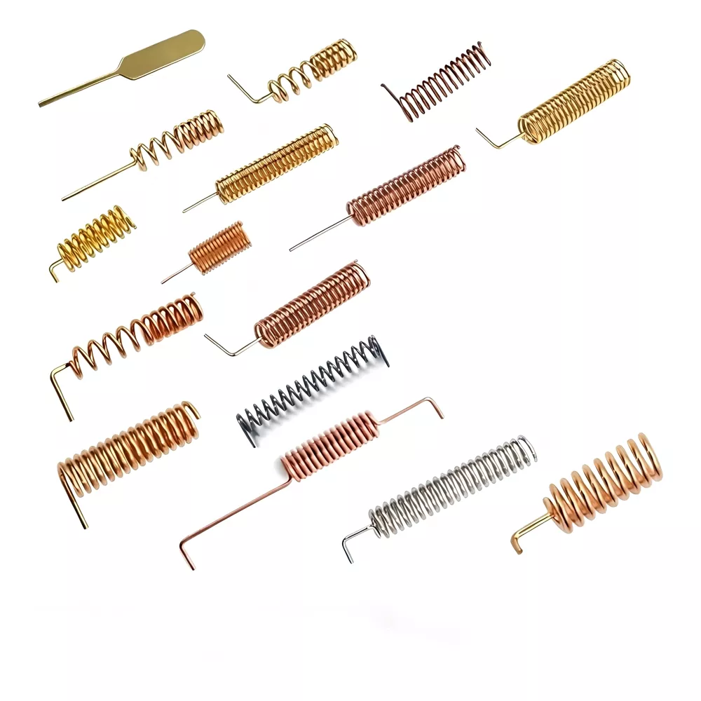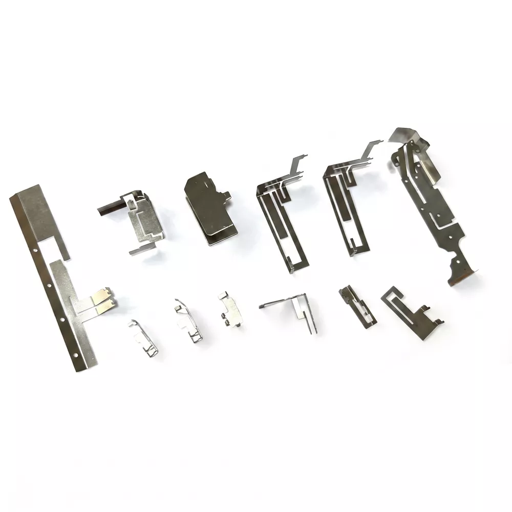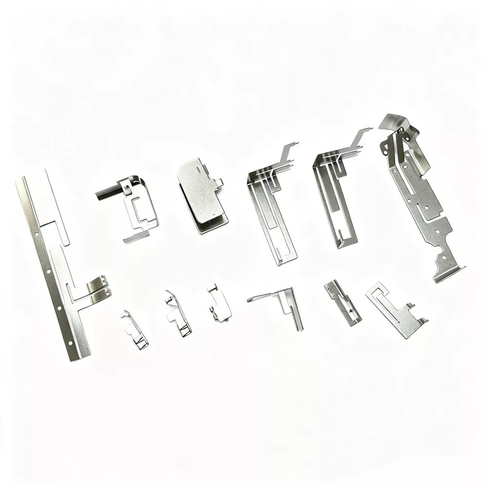
LDS Antenna
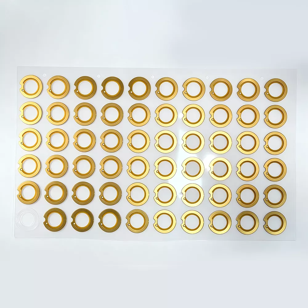
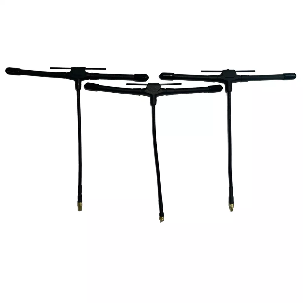
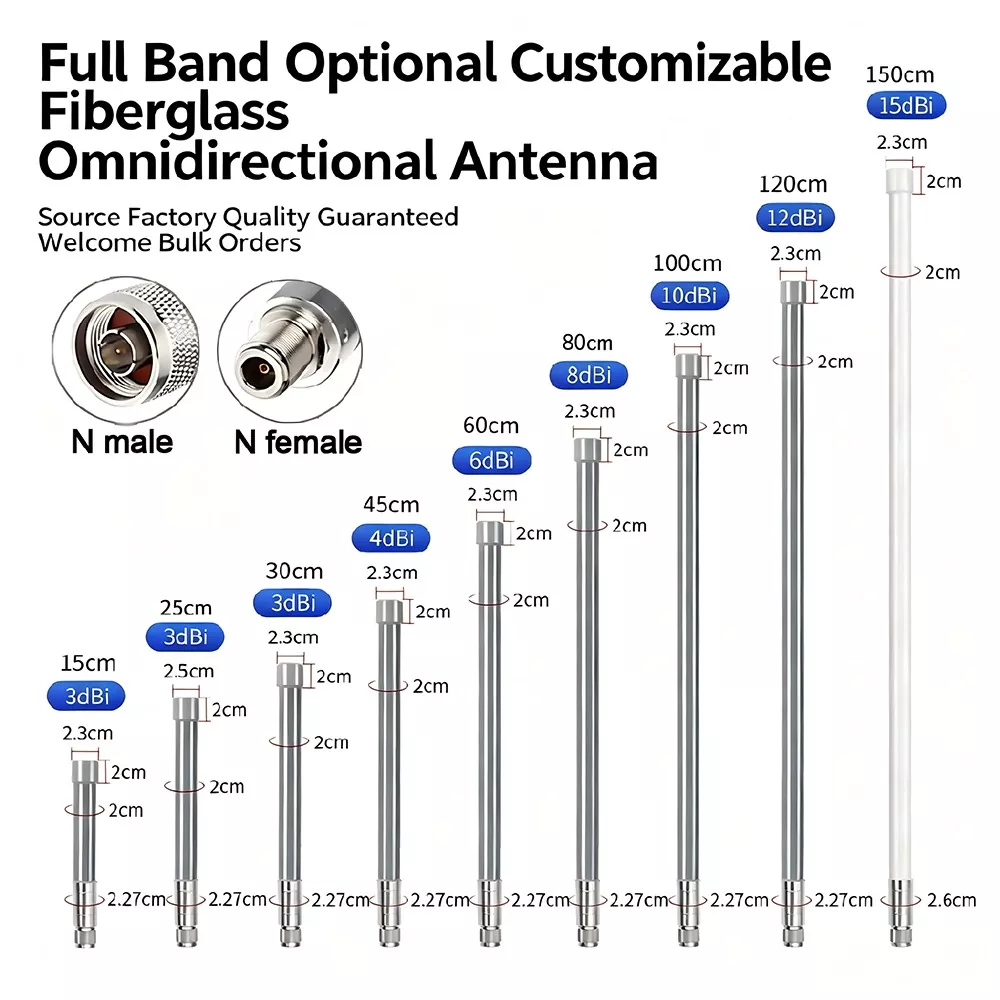
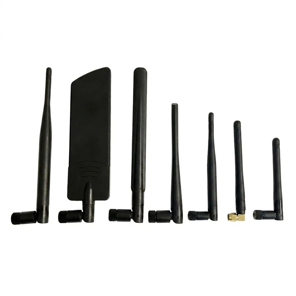
Looking for a reliable LDS Antenna Supplier in China? Shenzhen Qianmu Communication Technology is a professional manufacturer dedicated to high-quality 3D laser antennas. Direct from our factory, we offer cost-effective, space-saving antenna solutions with fast prototyping. Choose a verified China factory for your next antenna project and ensure top-tier RF performance.
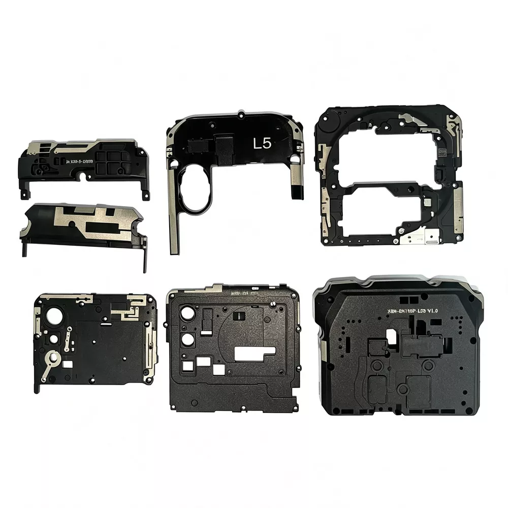
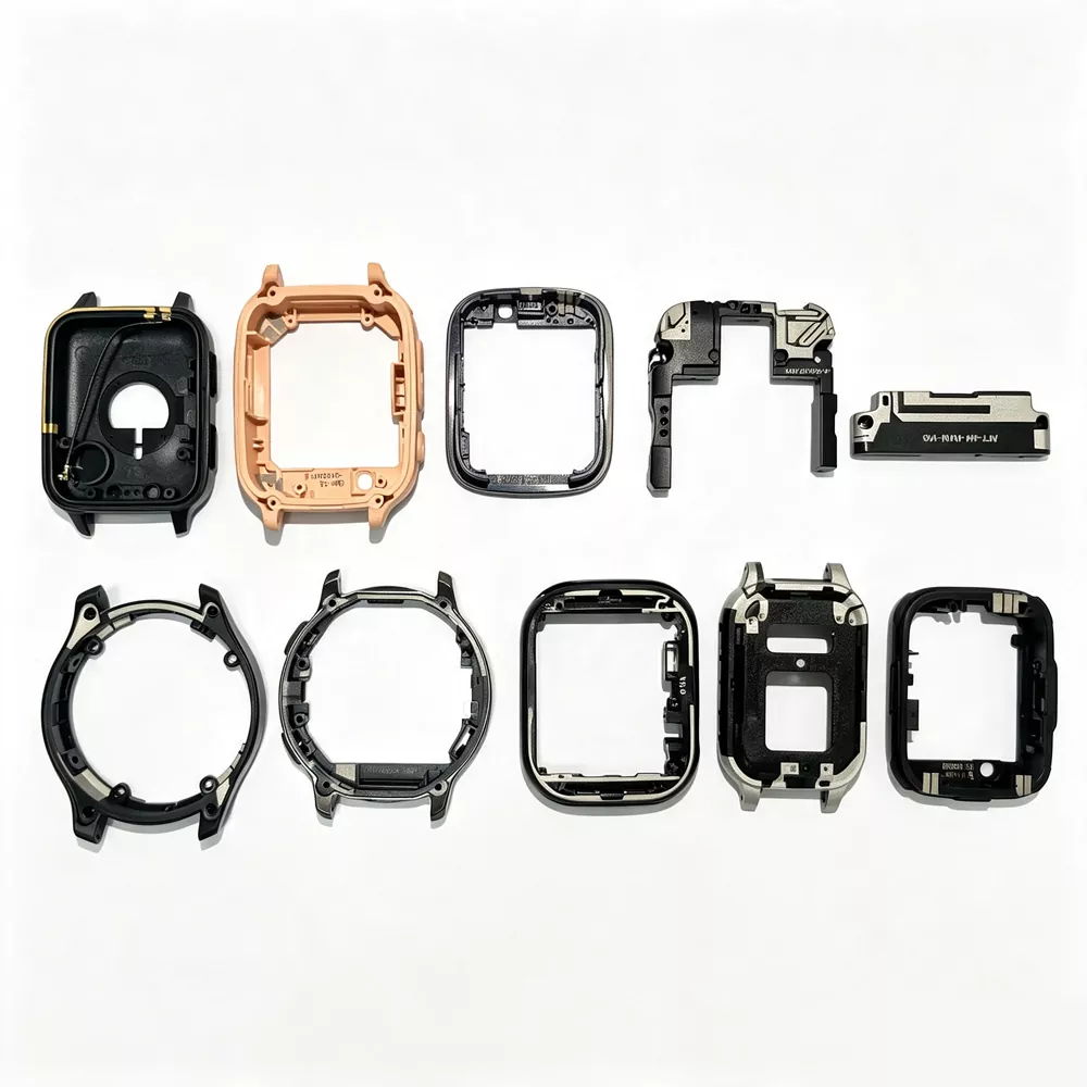
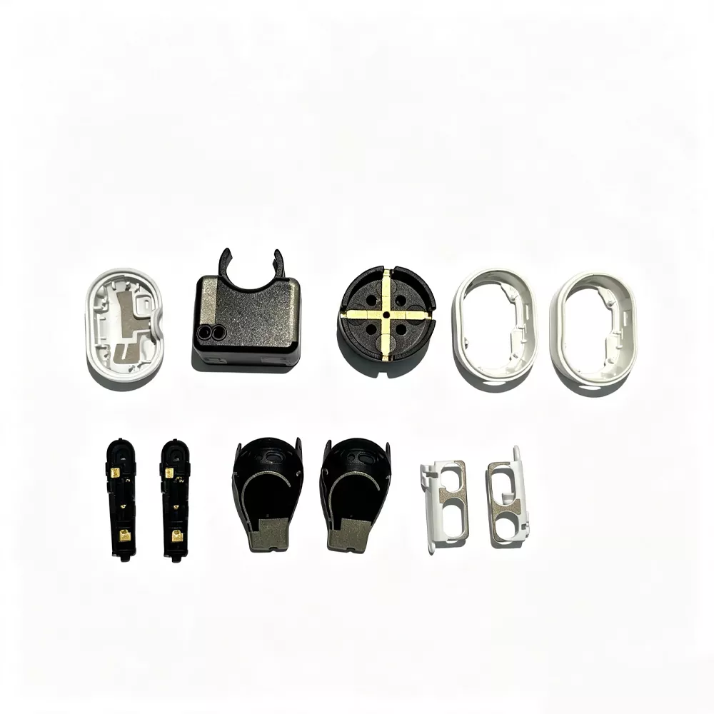
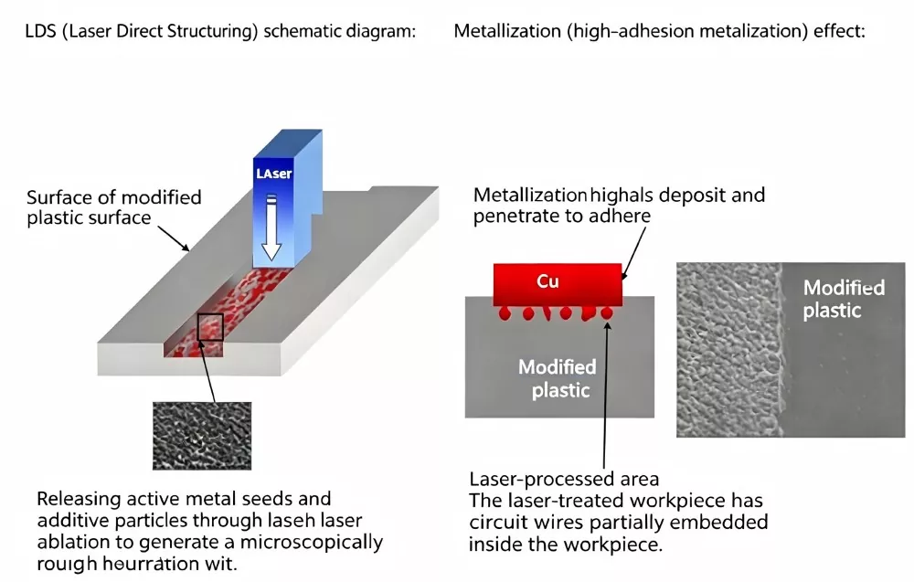
LDS Antenna (Laser Direct Structuring Antenna) is a 3D-MID-based RF structure manufactured by applying laser activation on injection-molded plastic substrates, followed by selective chemical plating to form conductive antenna traces.
The process enables conductive patterns to be directly defined on three-dimensional housing components, where antenna geometry is embedded into the mechanical structure rather than assembled as a separate RF part.
Unlike conventional stamped or sheet metal antennas that require discrete mounting inside the device, LDS Antenna integrates the radiating structure into the enclosure or internal plastic frame, allowing the antenna path to follow complex 3D geometries while maintaining defined electrical characteristics.
From a system perspective, LDS technology belongs to 3D-MID (Three-Dimensional Molded Interconnect Device), where a single molded component can combine structural, conductive, and housing functions through selective metallization of laser-activated surfaces.
Working Principle
The manufacturing process of LDS antennas can be divided into four core steps:
Step 1 – Injection Molding: Using LDS-specific functional plastics (containing special metal-organic composite additives), a three-dimensional plastic bracket or housing is produced via injection molding.
Step 2 – Laser Activation: The computer controls the laser's movement according to the trajectory of the conductive pattern, projecting the laser onto the surface of the three-dimensional plastic component and activating the circuit pattern within seconds. In the areas irradiated by the laser, the additives are activated, creating a microscopically rough surface that is conducive to metal deposition.
Step 3 – Chemical Plating: Place the activated plastic parts into a chemical plating bath, where metals such as copper, nickel, and gold are selectively deposited onto the activated areas, forming conductive traces.
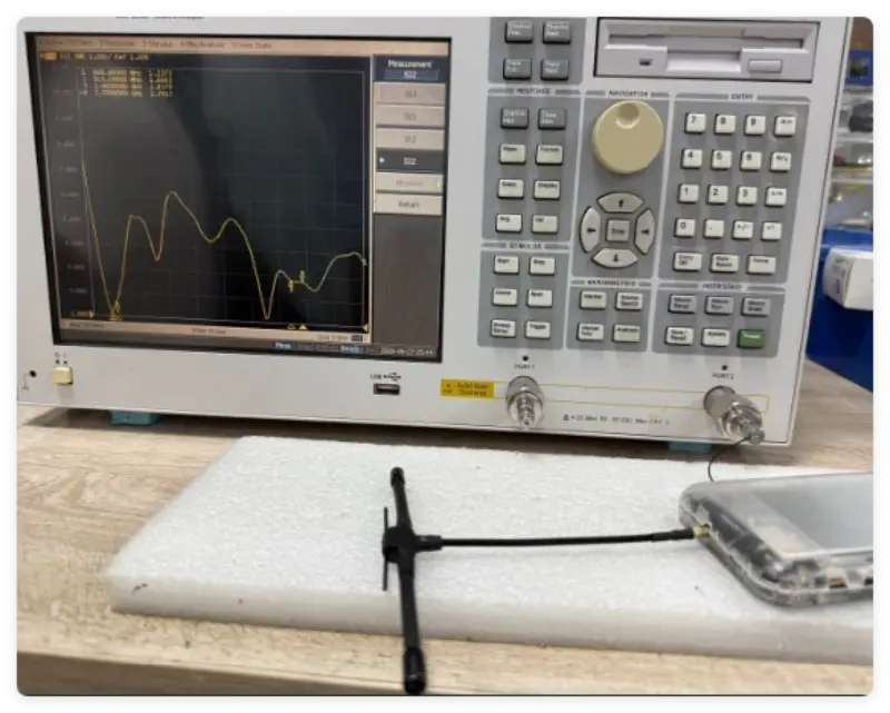
Step 4 – Assembly and Testing: The LDS housing for the antenna circuit is electrically connected to the PCB motherboard via spring contacts, pins, or B2B connectors. After a full inspection using a network analyzer, the assembly is delivered.
Applicable Devices
LDS antenna technology is widely used across multiple industries and wireless applications:
|
Industry |
Typical Applications |
|
Smartphones |
5G/4G mobile antennas, Wi-Fi / Bluetooth / GPS antennas, NFC payment modules |
|
Automotive Electronics |
eCall emergency communication antennas, TCU modules, V2X communication systems |
|
Wearable Devices |
Smartwatches, TWS earphones, AR/VR head-mounted devices |
|
Medical Devices |
Hearing aids, remote patient monitoring systems, portable medical terminals |
|
IoT Devices |
Asset tracking terminals, smart agriculture sensors, smart city infrastructure nodes |
|
Satellite Communication |
LEO satellite IoT terminals, GNSS positioning and navigation devices |
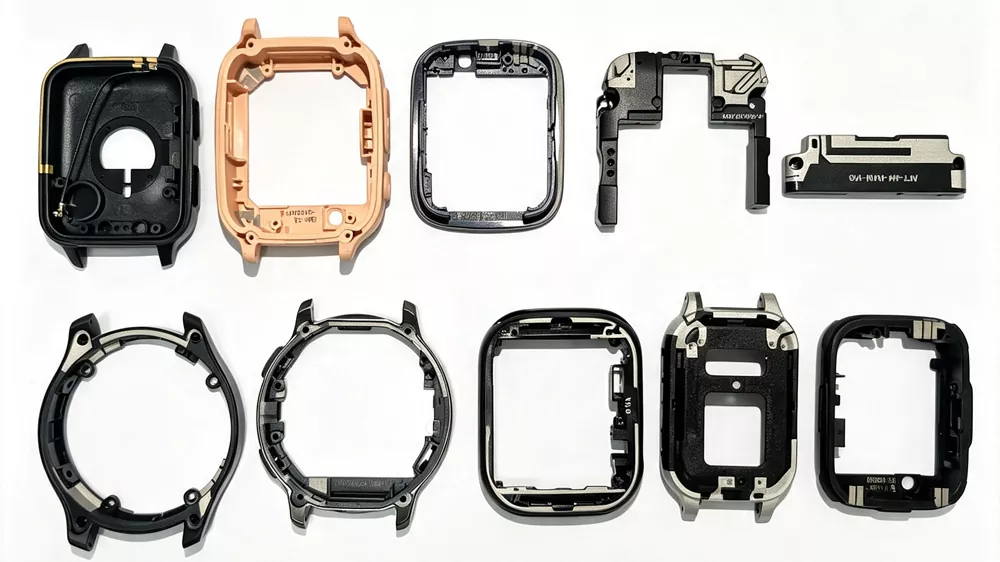
Core Selling Points
1. High space integration capability
LDS antennas can be integrated directly into device housings or structural brackets, enabling thinner product designs without significantly compromising RF performance. Antenna clearance is achieved through precise 3D patterning on plastic substrates, making it suitable for compact multi-band wireless devices.
2. Production stability and process consistency
Laser structuring provides high repeatability and stable pattern resolution, making it suitable for continuous production environments. Each unit is typically validated through RF testing, with key parameters such as S11 verified to ensure matching performance within design targets.
3. Reduced internal RF interference
Since conductive patterns are formed directly on the device housing, LDS structures reduce dependency on internal wiring and minimize interference caused by nearby metal components inside the enclosure.
4. Multi-band antenna integration capability
Multiple functional antennas (LTE / GSM / Wi-Fi / Bluetooth / GNSS) can be integrated onto a single 3D substrate, reducing overall component count and simplifying system-level RF architecture.
5. Flexible 3D RF design capability
LDS technology supports the implementation of complex conductive geometries on curved surfaces, allowing antenna layout to follow mechanical contours while maintaining defined RF constraints across different frequency bands.
Technical Specifications
|
Parameter |
Specification description |
|
Frequency range |
700MHz – 6 GHz (covers LTE700/GSM/WCDMA/LTE/5G Sub-6 GHz/Wi-Fi 2.4G/5G/GPS frequency bands) |
|
Impedance |
50Omega |
|
Peak gain |
1.6 – 2.2 dBi (depending on video segment and design) |
|
Average efficiency |
47% – 60% (depending on video segment and design) |
|
Rated power |
Up to 4W |
|
Operating temperature |
-40℃ ~ +85℃ |
|
Base material |
LDS-specific functional plastics (such as PC/ABS/LCP, etc.) |
|
Line accuracy |
Line width / Line spacing ≥ 0.1 mm |
|
Surface treatment |
Chemical copper plating + nickel/gold (customizable) |
Laser Engraving Process and Precautions
(1)Notes on Conductive Circuit Design
① Trace routing on LDS 3D substrates should avoid frequent sharp-angle transitions. On multi-face structures, continuous routing across adjacent surfaces generally improves process stability and plating uniformity, especially in larger housings.
② Minimum laser-defined trace width is typically around 0.2 mm, depending on design resolution and substrate geometry.
③ Minimum spacing between adjacent conductive traces is generally kept above 0.5 mm to reduce the risk of plating bridge formation during electrochemical deposition.
④ Clearance between conductive areas and enclosure boundaries is normally controlled at sub-millimeter scale. A buffer distance of approximately 1–2 mm near cavity walls is commonly applied to reduce edge contamination during laser processing.
⑤ Surface geometry influences plating behavior. Flat regions tend to provide more stable laser activation and coating consistency, while curved surfaces may introduce variation in thickness and adhesion due to angular exposure differences.
⑥ After laser structuring, parts are transferred directly to electroplating to minimize oxidation and surface contamination before metallization.
(2)LDS Product Storage Requirements Before Plating and Coating
① Laser-activated parts should be stored in controlled humidity conditions (typically below 60% RH) and transferred to plating as soon as process flow allows, to reduce surface oxidation risk.
② Direct contact with laser-processed surfaces is avoided, as contamination may affect subsequent metal deposition quality.
③ Dedicated trays or fixtures are used during handling and transport to maintain positional stability and prevent surface damage or micro-scratching.
Compare with peers
Quality Control Process
1. Incoming Material Inspection: Testing the Metal Additive Content in Plastic Particles Specifically Designed for LDS
2. Injection molding control: Dimensional accuracy ±0.05mm
3. Laser marking: AOI automated optical inspection for circuit integrity
4. Chemical plating: Coating thickness uniformity inspection (copper layer ≥ 5 μm, nickel/gold layer ≥ 0.1 μm)
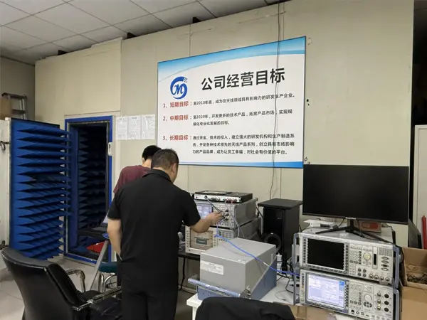
5. RF Testing: The network analyzer performs a full inspection of S11, VSWR, gain, and efficiency.
6. Reliability sampling inspection:Hundred gridAll-inclusive adhesion testing
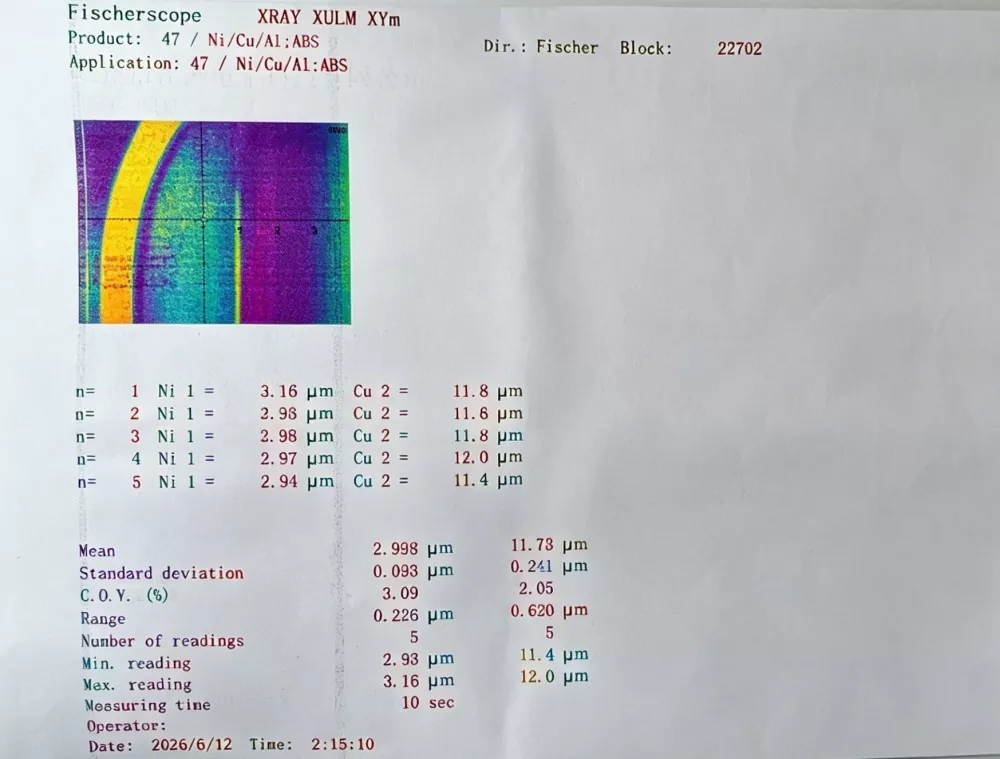
As a reliable supplier, each batch of our products comes with a test report that can be traced back to the corresponding raw material batch.
How to Choose LDS Antenna Products
1. View frequency band requirements
Clearly specify which communication frequency bands the device needs to support—2G/3G/4G/5G Sub-6GHz, Wi-Fi 2.4G/5G/6E, GPS/GNSS, Bluetooth, NFC, and others. Different frequency bands correspond to different antenna routing designs.
2. Check the installation space
- Does the device housing have sufficient LDS layout space?
- Does the antenna need to follow the routing along a 3D curved surface? That's precisely where LDS excels.
3. Check the substrate selection
The substrate material for LDS antennas must be an LDS-specific functional plastic. Common options include PC, ABS, PC+ABS, and LCP. Different materials have their own advantages and disadvantages in terms of temperature resistance, dielectric constant, and mechanical strength.
4. Check the lead time and minimum order quantity.
As a manufacturer, we offer:
- Sample stage:10Fast prototyping
- Small batch: 100–1,000 pcs, 2-week delivery
- Large-scale production: Monthly capacity exceeds 100,000 units, with guaranteed delivery times.
FAQ
Q: What's the difference between an LDS antenna and an FPC antenna?
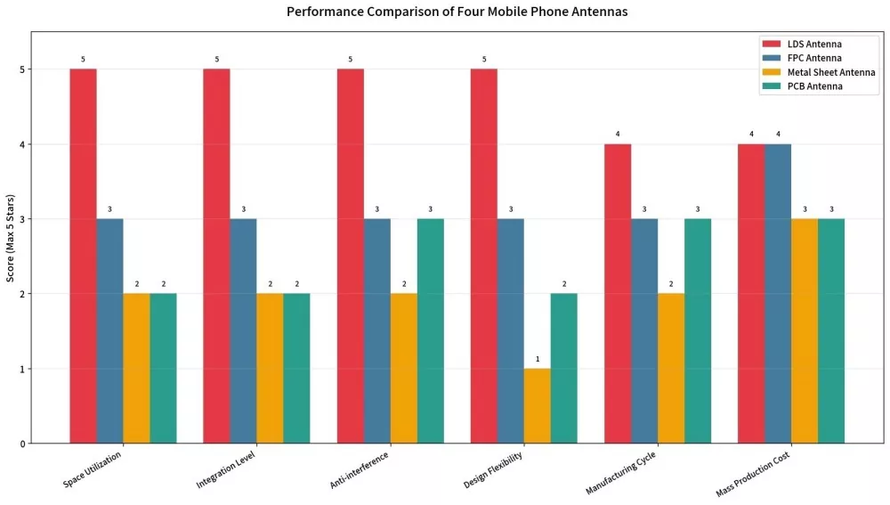
A: An FPC antenna is a flexible circuit solution installed inside the device, requiring dedicated planar space. An LDS Antenna is directly laser-structured onto the device housing or bracket, allowing better adaptation to 3D surfaces and improved space utilization. It also provides higher integration capability and stronger anti-interference performance compared with traditional FPC solutions.
Q: What is the minimum order quantity for customization?
A: No minimum order quantity is required during the sample stage. We support sample requests, small-batch production starting from 100 pcs, and larger-volume orders based on customer requirements. As a direct factory, we provide flexible production support throughout different project stages.
Q: What information is required for customization?
A: Customers can provide 3D CAD drawings of the device (STEP or IGS format), target frequency band, PCB layout, and connector type. Our engineering team will handle routing design, simulation optimization, and prototype verification.
Q: Can this technology support 5G millimeter-wave applications?
A: Yes. The technology supports antenna designs for both Sub-6 GHz and millimeter-wave frequency bands. The final solution will be optimized according to device structure, available space, and required frequency performance.
Q: What is the service life of the antenna?
A: Reliability tests show that after 100 thermal cycles from -40℃ to +85℃ and high-temperature/high-humidity testing at 85℃/85% RH for 168 hours, performance degradation remains below 5% while adhesion remains stable. The designed service life can exceed 10 years.
Q: Can you provide antenna tuning support?
A: Yes. We provide complete tuning services, including simulation, prototyping, and system-level optimization, helping products meet certification requirements such as CTA, CE, and FCC.
Hot Tags: LDS Antenna Manufacturer, Custom, Wholesale
Related Category
Send Inquiry
Contact Info
-
Address
Hangcheng High-tech Industrial Park, Hangkong Road, Sanwei Community, Hangcheng Subdistrict, Bao'an District, Shenzhen City, Guangdong Province, China
-
Tel
-
E-mail
Contact Qianmu Communication for professional antenna solutions and customized manufacturing services. As a reliable antenna manufacturer, supplier and factory in China, we provide technical consultation, product customization, sample testing and production support for customers worldwide.